Light Speed Ahead: Photonic Chips Are Leaving the Lab and Coming for Silicon's Crown
Silicon has had a pretty good run. Decades of Moore's Law scaling turned a beach sand derivative into the foundation of the entire digital world. But physics has a way of eventually catching up with engineering ambition, and the walls that silicon transistors are running into — heat, power density, interconnect latency — are starting to look less like temporary obstacles and more like permanent ceilings.
Enter photonics. The idea of using light instead of electricity to process and move data has been floating around research labs since the 1980s. For most of that time, it stayed there — promising in theory, brutal in practice. But something has shifted in the last couple of years. The gap between "interesting research" and "shippable product" has closed dramatically, and 2025 is shaping up to be the year photonic computing stops being a punchline and starts being a genuine threat to conventional silicon.
Why Light Beats Electrons for Certain Problems
To understand why photonics is getting so much attention right now, it helps to understand what electrons are actually bad at. Moving electrical signals through copper wires and silicon traces generates heat, consumes power, and introduces latency that compounds as chip complexity grows. At the scale of a modern AI accelerator or a high-bandwidth network switch, these aren't minor inefficiencies — they're fundamental architectural constraints.
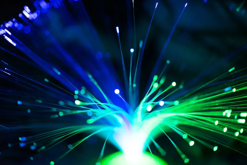
Photons don't have those problems in the same way. Light-based signals travel faster, generate far less heat in transit, and can carry multiple data streams simultaneously through wavelength multiplexing — essentially running different colors of light through the same waveguide at the same time. For data-intensive workloads like AI inference, matrix multiplication, and high-speed networking, those properties translate directly into performance and efficiency advantages that electronics simply can't match at equivalent scale.
The catch, historically, has been integration. Getting photonic components to work reliably at chip scale, and especially getting them to interface cleanly with conventional electronics, has been an engineering nightmare. That's the problem that's been cracking open over the last 18 months.
The 2024-2025 Breakthrough Moment
A few developments have genuinely changed the trajectory here. The first is silicon photonics manufacturing maturity. Major fabs — including GlobalFoundries and TSMC — have refined their silicon photonics processes to the point where photonic components can be fabricated using modified versions of standard CMOS workflows. That's huge. It means photonic chip production doesn't require entirely separate manufacturing infrastructure, which was one of the biggest barriers to cost-competitive scaling.
The second is co-packaging. Advanced packaging techniques that place photonic and electronic components in extremely close proximity — sometimes on the same substrate — have dramatically reduced the penalty of converting between optical and electrical signals. That conversion, known as the electro-optic interface, used to eat up a significant chunk of the efficiency gains photonics promised. Tighter integration has changed that calculus.
And then there are the companies actually shipping hardware. Lightmatter, based out of Boston, has been making waves with its Passage interconnect platform — a photonic chip-to-chip communication fabric that's already being evaluated by hyperscalers for data center deployments. Their pitch is essentially that you can keep your existing compute chips but replace the copper interconnects between them with optical links, cutting power consumption and boosting bandwidth simultaneously. That's a much easier sell than asking customers to rip out their entire compute stack.
Luxtera (acquired by Cisco), Intel's Silicon Photonics division, and a stealth-mode outfit called Ayar Labs are all pushing similar photonic interconnect strategies, while companies like Luminous Computing and Optalysys are going further — building processors where the actual computation happens in the optical domain, not just the communication.
Where Photonics Wins Right Now
It's worth being honest about where photonic computing has clear advantages today versus where it's still catching up.
For AI inference specifically, photonics looks genuinely compelling. Matrix-vector multiplication — the core mathematical operation in neural network inference — maps extremely well onto optical hardware. Analog photonic processors can perform these operations at the speed of light with power consumption that's orders of magnitude lower than equivalent digital silicon implementations. For companies running inference at massive scale, that efficiency delta is worth a lot of money.
High-performance networking and data center interconnects are another strong fit. The bandwidth density and energy efficiency of optical links at short distances (rack-to-rack, chip-to-chip) are already better than copper in many configurations, which is why optical transceivers have been a data center staple for years. Integrating that optical layer directly into compute packages is the next logical step.
General-purpose computing is harder. The programmability and flexibility of digital silicon is tough to replicate in optical systems, and the error correction challenges in analog photonic processors are real. Nobody is suggesting your next laptop will have a photonic CPU. But for specific, high-value workloads? The case is getting stronger fast.
The Five-Year Horizon
Here's where things get speculative, but productively so. If silicon photonics manufacturing continues maturing at its current pace, and if the co-packaging techniques being refined by companies like Ayar Labs hit their roadmap targets, the next five years could look something like this:
By 2026, photonic interconnects become standard in high-end AI inference servers and top-tier networking hardware. The power savings alone will drive adoption even among customers who aren't excited about the underlying technology.
By 2027-2028, hybrid photonic-electronic processors start appearing in cloud data centers — chips where optical components handle the bandwidth-intensive parts of the compute graph and traditional silicon handles the control logic and programmable elements. Think of it as a division of labor that plays to each technology's strengths.
By 2029-2030, if the analog photonic computing companies deliver on their roadmaps, we could see purpose-built photonic AI accelerators in production at multiple hyperscalers. The "transistor-to-photon" transition won't happen overnight, but the inflection point may be closer than most people in the industry are publicly willing to say.
What Early Adopters Should Watch
If you're tracking this space, a few things are worth keeping on your radar. Watch Lightmatter's customer announcements — any hyperscaler publicly endorsing their Passage platform would be a significant signal. Follow Intel's silicon photonics roadmap, since their fab access gives them scale advantages that pure-play photonics startups can't easily match. And keep an eye on DARPA funding flows; the agency has been a consistent early backer of photonic computing research, and where DARPA money goes, commercial development often follows within a decade.
The transistor revolutionized computing by giving engineers a reliable, scalable way to switch electrical signals. Photonics might be about to do something similar for an era where data volume and energy efficiency are the defining constraints. The lab era is over. The interesting part is just getting started.