Smashing the Memory Wall: The Bandwidth Revolution That Could Finally Let AI Models Run Free
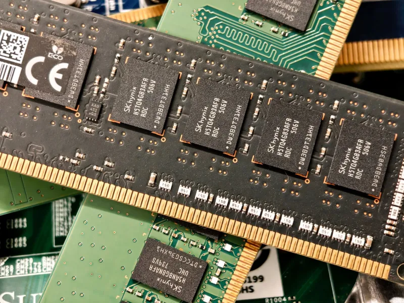
Here's a problem that doesn't get nearly enough airtime outside of hardware engineering circles: your GPU can crunch numbers at a blistering pace, but it spends a shocking amount of time just waiting. Waiting for data to arrive from memory. Waiting for weights to load. Waiting for activations to shuffle back and forth across a bus that was never really designed for what we're asking it to do in 2025.
That gap—between how fast silicon can compute and how fast memory can actually feed it—is called the memory wall. And right now, it's one of the most consequential bottlenecks in the entire AI ecosystem. The good news? Engineers are finally throwing serious hardware innovation at it, and the solutions emerging from labs and fabs across the country are genuinely exciting.
Why the Memory Wall Got So Bad, So Fast
For decades, compute performance scaled faster than memory bandwidth. That was fine when workloads were relatively modest. But modern large language models and multimodal AI systems are parameter-hungry beasts. A frontier model with hundreds of billions of parameters needs to constantly stream weights in and out of memory during inference—sometimes multiple times per forward pass.
High Bandwidth Memory (HBM) was supposed to fix this. And to be fair, HBM2e and HBM3 have been genuine improvements, offering bandwidth figures that would've seemed absurd ten years ago. But model sizes have scaled faster than HBM generations can keep up with. NVIDIA's H100, for example, delivers around 3.35 terabytes per second of memory bandwidth—impressive, but still a limiting factor when you're running a 70-billion-parameter model at enterprise inference loads.
The math just doesn't work in memory's favor right now. Compute FLOPS have scaled roughly 3x per generation over the last few years. Memory bandwidth? Closer to 1.5x. That divergence is the memory wall, and it's been getting taller.
Chiplets Are Changing the Geometry of the Problem
One of the most promising architectural shifts happening right now is the move toward chiplet-based designs. Instead of building one massive monolithic die, chiplet architectures break processors into smaller, specialized tiles that can be mixed, matched, and interconnected at close range.
What does that have to do with memory bandwidth? Quite a bit, actually. When you place memory logic chiplets physically adjacent to compute chiplets—connected through high-density die-to-die interconnects—you dramatically shrink the distance data has to travel. Shorter distance means lower latency and higher effective bandwidth, often without needing to push raw HBM specs any further.
AMD has been pioneering this space with its 3D V-Cache technology, and while that's primarily a CPU play, the underlying principle is migrating hard into AI accelerator design. Startups like Cerebras and established players like Intel are exploring similar ideas with their own tile-based and wafer-scale approaches. The common thread: get memory closer to compute, physically and architecturally.
3D Stacking Is Getting Serious
If chiplets are about horizontal integration, 3D stacking is about going vertical—literally stacking memory dies on top of compute dies using through-silicon vias (TSVs) or hybrid bonding. This isn't brand new, but the precision and yield improvements in 2024 and 2025 have made it practical at a scale that wasn't realistic before.
The appeal is straightforward: by stacking SRAM or even DRAM directly on top of a compute tile, you can achieve bandwidth densities that blow traditional HBM out of the water for on-chip workloads. Some research implementations have demonstrated effective bandwidths exceeding 10 terabytes per second for specific access patterns—figures that would fundamentally change how attention mechanisms in transformer models behave at runtime.
Samsung, SK Hynix, and Micron are all racing on this front. SK Hynix's HBM3E, already shipping to select customers, is a stepping stone, but the real prize is processing-in-memory (PIM) architectures where compute logic lives inside the memory stack itself. That's a paradigm shift, not just an incremental bump.
Coherent Memory Protocols: The Software Side of the Fix
Hardware alone won't solve this. One of the underappreciated contributors to memory inefficiency is the lack of coherent memory protocols across heterogeneous compute environments. When a CPU, GPU, and AI accelerator all need to access the same data, you end up with redundant copies, synchronization overhead, and cache thrashing that eats into effective bandwidth.
CXL—Compute Express Link—is the industry's best current answer to this. CXL 3.0, which started appearing in production systems late in 2024, enables coherent memory pooling across multiple processors and accelerators over a PCIe physical layer. For AI training clusters, this means workloads can dynamically share a unified memory pool rather than maintaining separate, siloed memory spaces on each accelerator.
The enterprise implications here are significant. Coherent memory pools let you run larger effective batch sizes, reduce the frequency of expensive data movement operations, and simplify the programming model for distributed training jobs. Microsoft's Azure and Google Cloud have both been quietly integrating CXL-capable infrastructure, and on-premises AI clusters are starting to follow.
What This Means for Model Training and Inference in Practice
Let's ground this in something concrete. A company running a fine-tuning pipeline on a 13-billion-parameter model today is likely spending a meaningful fraction of GPU time in memory-bound operations. Better bandwidth architectures don't just speed things up marginally—they can shift the entire performance profile of a training run.
For inference specifically, the impact is even more direct. Latency-sensitive applications like real-time coding assistants, customer service AI, or medical diagnostic tools live and die by how fast a model can generate tokens. Memory bandwidth is often the primary constraint on tokens-per-second throughput at production scale. Closing the memory-compute gap by even 30–40% could translate directly into lower inference costs and snappier user experiences.
Startups building inference infrastructure—companies like Groq, with its deterministic LPU architecture, or Etched, designing chips purpose-built for transformer inference—are already baking these memory bandwidth principles into their silicon from the ground up rather than retrofitting them onto GPU architectures that were designed for a different era.
The Road Ahead
None of this is a solved problem yet. 3D stacking at scale still faces yield and thermal challenges. CXL adoption is moving, but it's not ubiquitous. Chiplet interconnects are powerful but add design complexity that not every team can absorb.
But the trajectory is clear, and it's moving fast. The memory wall that's been quietly throttling AI model scaling for the past few years is finally getting the serious engineering attention it deserves. By 2026, the combination of heterogeneous chiplet designs, stacked memory, and coherent pooling protocols could look less like a wall and more like a speed bump.
For early adopters and enterprise AI teams planning hardware investments right now, understanding this landscape isn't optional—it's the difference between buying into yesterday's bottleneck and positioning for what compute actually looks like on the other side of it.